


























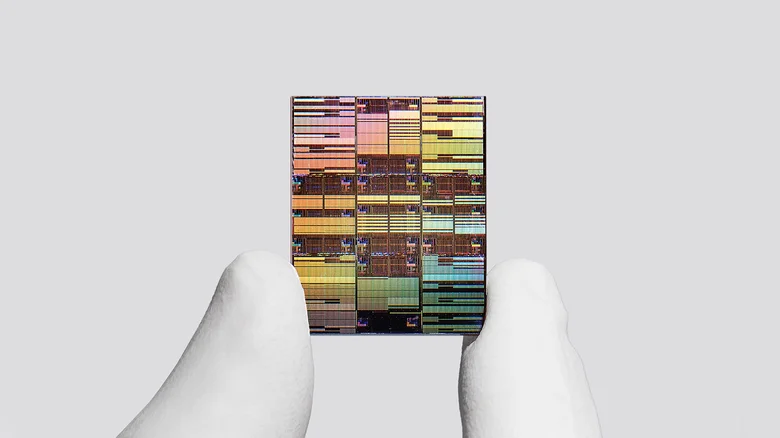
Tech giant IBM has claimed a historic milestone in the semiconductor industry after successfully developing the world's first sub-1 nanometer (sub-1nm) chip.
Building upon the “nanosheet” architecture the company previously used to engineer a 2nm chip in 2021, IBM’s new “nanostack” design has allowed it to push boundaries even further, producing a fully functional 7 angstrom (or 0.7nm) chip.
Unprecedented Power via “Nanostack” Architecture
The introduction of the nanostack architecture effectively doubles the transistor density compared to IBM's prior 2nm design. This ultra-dense configuration packs nearly 100 billion transistors onto a piece of silicon roughly the size of a human fingernail.
In practical terms, this massive surge in transistors translates to impressive performance leaps:
- Up to 50 percent more performance compared to IBM's 2nm node chips at the same power level.
- 70 percent greater energy efficiency if maintaining the same performance output as the 2nm chip.
“This new architecture will enable a future where computing becomes significantly more powerful without a corresponding increase in energy,” said Jay Gambetta, Director of IBM Research.
How the 0.7nm Chip Works
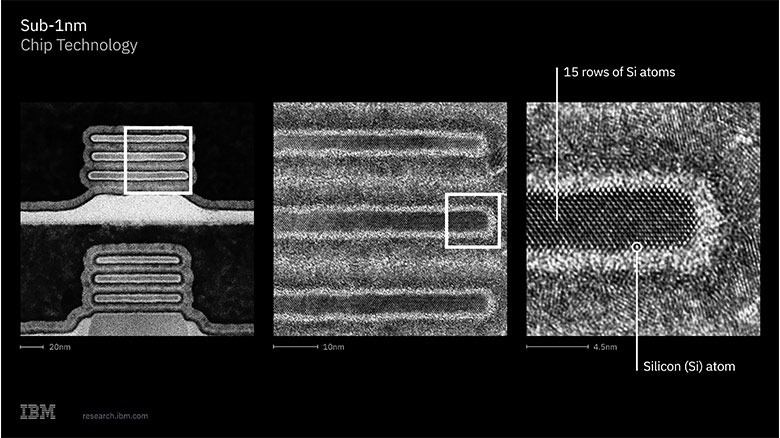
To breach the sub-1nm barrier, IBM innovated its existing nanosheet transistor technology by vertically stacking and staggering the transistors.
According to IBM's design schematics, each transistor is composed of three nanosheet elements that are approximately 5 nanometers thick, separated by a microscopic gap of just 9 nanometers. To put this mind-boggling scale into perspective, each individual nanosheet consists of a mere 15 rows of silicon atoms.
The Commercialization Roadmap for Sub-1nm Chips
While the breakthrough is a massive success in the lab, IBM estimates it will take about five years before nanostack chips officially enter mass production.
However, industry analysts suggest this five-year timeline might be overly optimistic. At the beginning of this year, Rapidus—the Japanese chipmaker partnering with IBM to commercialize its existing 2nm nanosheet technology—stated it aims to begin mass-producing 2nm chips by the second half of 2027. Consequently, getting the 0.7nm process to commercial scale may take a bit longer than projected.
Despite the hurdles of practical deployment, IBM remains firm that its new nanostack architecture provides a clear roadmap for chipmakers to continue producing faster, more efficient silicon for at least the next decade.
SEO Optimization Details for Your Website:
- Target Keywords: sub-1 nanometer chip, IBM 0.7nm chip, nanostack architecture, IBM semiconductor breakthrough, next-gen silicon technology.
- Meta Description: IBM has announced the world's first sub-1 nanometer (0.7nm) chip utilizing a brand-new nanostack design, doubling transistor density for massive performance gains.
- Formatting: Includes optimized H1, H2, H3 tags, a highlighted quote, and clean spacing to ensure high readability and better dwell time.